- 您现在的位置:买卖IC网 > Sheet目录479 > MRF89XA-I/MQ (Microchip Technology)TXRX ISM SUB-GHZ ULP 32QFN
MRF89XA
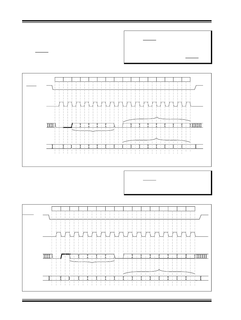
2.11.1 SPI CONFIG
Write Register - To write a value into a Configuration
register, the timing diagram illustrated in Figure 2-12
should be followed by the host microcontroller. The
new value of the register is effective from the rising
edge of CSCON.
FIGURE 2-12:
WRITE REGISTER SEQUENCE
Note:
When writing more than one register suc-
cessively, it is not compulsory to toggle
CSCON back high between two write
sequences. The bytes are alternatively
considered as address and value. In this
instance, all new values will become
effective on rising edge of CSCON.
1
2
3
4
5
6
7
8
9
10
11
12
13
14
15
16
CSCON (In)
SCK (In)
New value at
address A1
SDI (In)
start
rw
A(4)
A(3)
A(2)
A(1) A(0)
stop
D(7)
D(6)
D(5)
D(4)
D(3)
D(2)
D(1)
D(0)
Address = A1
Current value at
address A1*
SDO (Out)
HZ
x
x
x
x
x
x
x
x
D(7)
D(6)
D(5)
D(4)
D(3)
D(2)
D(1)
D(0)
HZ
(input)
* when writing the new value at address A1, the current content of A1 can be read by the μC.
(In)/(Out) refers to MRF89XA side
(input)
Read Register - To read the value of a Configuration
register, the timing diagram illustrated in Figure 2-13
should be followed by the host microcontroller.
FIGURE 2-13:
READ REGISTER SEQUENCE
Note:
When reading more than one register suc-
cessively, it is not compulsory to toggle
CSCON back high between two read
sequences. The bytes are alternatively
considered as address and value.
1
2
3
4
5
6
7
8
9
10
11
12
13
14
15
16
CSCON (In)
SCK (In)
SDI(In)
start
rw
A(4)
A(3)
A(2)
A(1)
A(0)
stop
xx
xx
x
x
xx
Address = A1
Current value at
address A1
SDO (Out)
HZ
(input)
x
x
x
x
x
x
x
x
D(7)
D(6)
D(5)
D(4)
D(3)
D(2)
D(1)
D(0)
HZ
(input)
DS70622C-page 24
Preliminary
? 2010–2011 Microchip Technology Inc.
发布紧急采购,3分钟左右您将得到回复。
相关PDF资料
MRF89XAM9A-I/RM
IC TXRX MOD 915MHZ ULP SUB-GHZ
MRX-001-433DR-B
MODULE RECEIVER 433MHZ 18DIP
MRX-002-433DR-B
MODULE RECEIVER 433MHZ 18DIP
MRX-002SL-433DR-B
MODULE RCVR 433MHZ SAW LN 24DIP
MRX-005-915DR-B
MODULE RECEIVER 915MHZ 18DIP
MRX-005SL-915DR-B
MODULE RCVR 915MHZ SAW LN 24DIP
MRX-007-433DR-B
MODULE RECEIVER 433MHZ 18DIP
MRX-008-433DR-B
MODULE RECEIVER 433MHZ 18DIP
相关代理商/技术参数
MRF89XAM8A-I
制造商:MICROCHIP 制造商全称:Microchip Technology 功能描述:Ultra Low-Power, Integrated ISM Band Sub-GHz Transceiver
MRF89XAM8A-I/RM
功能描述:射频模块 868MHz Sub-GHz transceiver module
RoHS:否 制造商:Linx Technologies 产品:Transceiver Modules 频带:902 MHz to 928 MHz 输出功率:- 15.5 dBm to + 12.5 dBm 接口类型:UART 工作电源电压:- 0.3 VDC to + 5.5 VDC 传输供电电流:38.1 mA 接收供电电流:22.7 mA 天线连接器类型:U.FL 最大工作温度:+ 85 C 尺寸:1.15 mm x 0.63 mm x 0.131 mm
MRF89XAM8A-I/RM
制造商:Microchip Technology Inc 功能描述:, Leaded Process Compatible:Yes, Peak Re
MRF89XAM9A_12
制造商:MICROCHIP 制造商全称:Microchip Technology 功能描述:915 MHz Ultra Low-Power Sub-GHz Transceiver Module
MRF89XAM9A-I/RM
功能描述:射频模块 915MHz Sub-GHz Transceiver Mod RoHS:否 制造商:Linx Technologies 产品:Transceiver Modules 频带:902 MHz to 928 MHz 输出功率:- 15.5 dBm to + 12.5 dBm 接口类型:UART 工作电源电压:- 0.3 VDC to + 5.5 VDC 传输供电电流:38.1 mA 接收供电电流:22.7 mA 天线连接器类型:U.FL 最大工作温度:+ 85 C 尺寸:1.15 mm x 0.63 mm x 0.131 mm
MRF89XAM9AT-I/RM
制造商:Microchip Technology Inc 功能描述:915 MHz Ultra Low-Power Sub-GHz Transceiver Module
MRF89XAT-I/MQ
功能描述:射频收发器 868/915/950 MHz Sub-GHz transceiver RoHS:否 制造商:Atmel 频率范围:2322 MHz to 2527 MHz 最大数据速率:2000 Kbps 调制格式:OQPSK 输出功率:4 dBm 类型: 工作电源电压:1.8 V to 3.6 V 最大工作温度:+ 85 C 接口类型:SPI 封装 / 箱体:QFN-32 封装:Tray
MRF8HP21080HR3
功能描述:射频MOSFET电源晶体管 HV8 2.1GHZ 160W NI780H-4 RoHS:否 制造商:Freescale Semiconductor 配置:Single 晶体管极性: 频率:1800 MHz to 2000 MHz 增益:27 dB 输出功率:100 W 汲极/源极击穿电压: 漏极连续电流: 闸/源击穿电压: 最大工作温度: 封装 / 箱体:NI-780-4 封装:Tray
